Contents
Diodes(Number and Coding schemes)
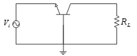
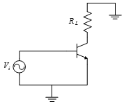
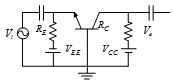
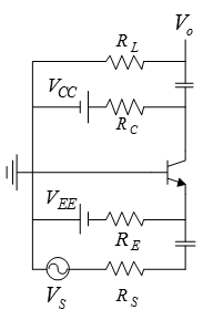
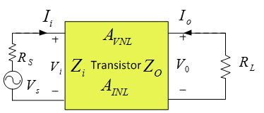
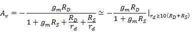
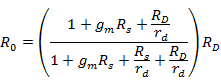
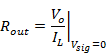
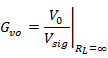
Effect of Source & Load Resistance
Summary of Single Stage BJT Amplifiers
Effect of Source & Load Resistance
Frequency Response of BJT Amplifiers
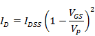
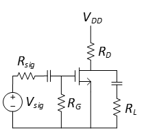
JFET (Junction Field Effect Transistor)
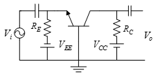
Single stage amplifiers without source and load resistance
Summary of Single Stage BJT Amplifiers
There are a number of common, standard and manufacturer-driven numbering and coding schemes for diodes; the two most common being the EIA/JEDEC standard and the European Pro Electron standard
EIA/JEDEC
A standardized 1N-series numbering system was introduced in the US by EIA/JEDEC (Joint Electron Device Engineering Council) about 1960. Among the most popular in this series were: 1N34A/1N270 (Germanium signal), 1N914/1N4148 (Silicon signal), 1N4001-1N4007 (Silicon 1A power rectifier) and 1N54xx (Silicon 3A power rectifier)
Pro Electron
The European Pro Electron coding system for active components was introduced in 1966 and comprises two letters followed by the part code. The first letter represents the semiconductor material used for the component (A = Germanium and B = Silicon) and the second letter represents the general function of the part (for diodes: A = low-power/signal, B = Variable capacitance, X = Multiplier, Y = Rectifier and Z = Voltage reference), for example:
· AA-series germanium low-power/signal diodes (e.g.: AA119)
· BA-series silicon low-power/signal diodes (e.g.: BAT18 Silicon RF Switching Diode)
· BY-series silicon rectifier diodes (e.g.: BY127 1250V, 1A rectifier diode)
· BZ-series silicon Zener diodes (e.g.: BZY88C4V7 4.7V Zener diode)

· PIV is the maximum voltage that a reverse biased can withstand without going into avalanche breakdown
|
Type of rectifier |
Peak Inverse Voltage |
Diagram |
|
Half wave rectifier |
|
|
|
Full wave rectifier |
|
|
|
CT Full waver rectifier |
|
|
![]() is the peak of the input
sinusoidal.
is the peak of the input
sinusoidal.
|
Saturation current Emission coefficient Series resistance Junction capacitance Transit time Reverse bias breakdown voltage Reverse bias breakdown current
|
|
Zener Diode V- I Characteristics |
|
||||
|
ON and OFF states of Zener Diode
|
|
||||
|
The Zener
potential is |
|


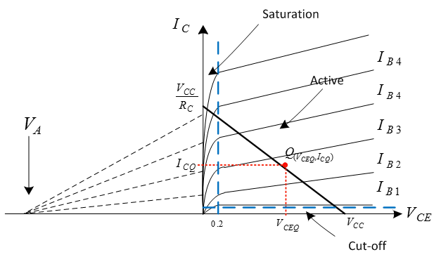
The
voltage ![]() gives the actual status of
the transistor in terms of saturation and active mode.
gives the actual status of
the transistor in terms of saturation and active mode.
|
Type |
|
Status |
|
NPN |
Negative |
Active |
|
PNP |
Positive |
Active |
|
Type |
|
Status |
|
NPN |
Positive |
Saturation |
|
PNP |
Negative |
Saturation |

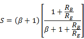
A transistor in saturation cannot amplify signals faithfully. Proper amplification takes place when transistor is in active mode.
|
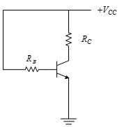
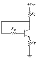
Fixed Bias |
|
|
|
|
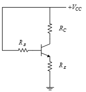
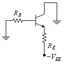
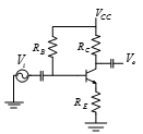
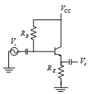
Emitter Bias |
|
|
|
|
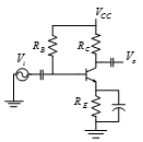
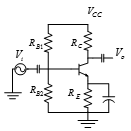
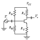
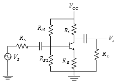
Voltage Divider Bias |
|
|
|
|
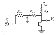
Collector Feedback Bias |
|
|
|
|
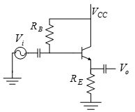
Emitter Follower Bias |
|
|
|

|
npn Common base |
|
|
||||||||
|
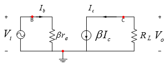
npn Common emitter |
|
|
|
|
|
|
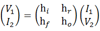
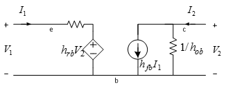
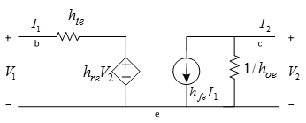
Hybrid Model |
Comparison
with |
||||||||||
|
Common Base |
|
|
||||||||||
|
Common Emitter |
|
|
||||||||||
|
Complete hybrid parameter with source and load resistance |
|
|
|
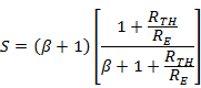
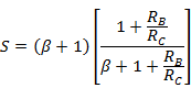
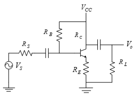
Common emitter Fixed Bias |
|
Common Emitter Collector Feedback Bias |
|
||||||||||||||||
|
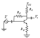
Common emitter Self Bias (unbypassed emitter) |
|
Common Emitter Collector Feedback Bias (unbypassed emitter)
|
|
||||||||||||||||
|
Common emitter Self Bias (bypassed emitter) |
|
Common Emitter Collector Feedback Bias (bypassed emitter)
|
|
||||||||||||||||
|
Common emitter Voltage Divider Bias (bypassed emitter)
|
|
Common emitter Voltage Divider Bias (unbypassed emitter)
|
|
||||||||||||||||
|
Common collector Self Bias |
|
Common base Fixed Bias |
|


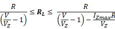
·
![]()
The
results for ![]() and
and ![]() change
if
change
if ![]() is taken
into account.
is taken
into account.
|
|
|
|
|
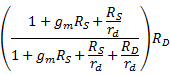
Calculation without (Ignoring the effect of |
Calculation with (Ignoring the effect of |
|
|
|
|
|
|
|
|
|
|
|
|
|
|
|
|
|
|
|
||
|
|
Calculation without (Ignoring the effect of |
Calculation with (Ignoring the effect of |
|
|
|
|
|
|
|
|
|
|
|
|
|
|
|
|
|
|
|
|
|
|
|
|
|
|
Calculation without (Ignoring the effect of |
Calculation with (Ignoring the effect of |
|
|
|
|
|
|
|
|
|
|
|
|
|
|
|
|
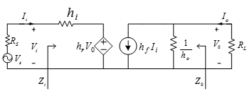
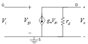
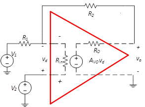
Let us assume that a transistor has the following small signal parameters:
|
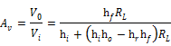
Voltage Gain |
|
|
Current Gain |
|
|
Input Impedance |
|
|
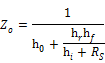
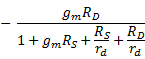
Output Impedance |
|
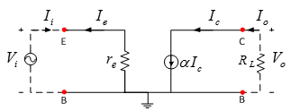
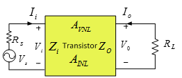
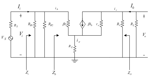
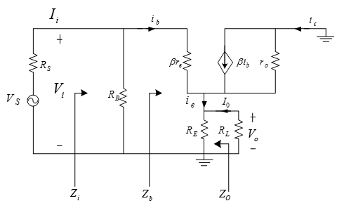
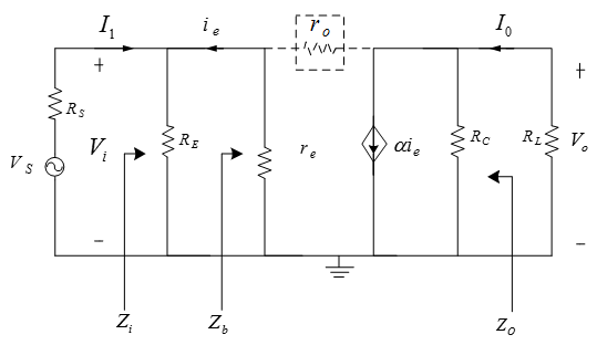
These parameters are used to model a two port network from which the effect of source and load resistance is found out.
![Machine generated alternative text:
]RL](Analog%20Circuits_files/image145.png)
|
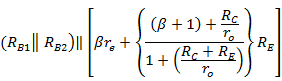
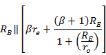
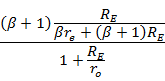
Effect
of source resistance |
|
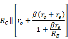
|
Effect
of source resistance |
|
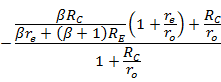
|
Effect
of source resistance |
|
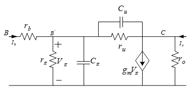
· Also known as Giacoletto model
· Complete model for low and high frequencies.
·
At low frequencies ![]() and
and ![]() models are used for
calculation simplicity.
models are used for
calculation simplicity.
|
|
Base contact + Base bulk + Base spreading resistance |
|
|
|
|
usual input resistance of CE |
|
|
|
very high in |
|
|
|
(10-40) |
|
|
|
transconductance |
|
|
|
|
|
|
|
|
*u subscript stands for union between base and collector.
|
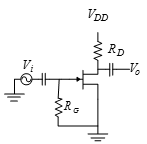
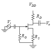
Common Emitter Self Bias Voltage Divider |
|
|
||||||||
|
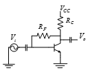
Common Emitter Collector Feedback |
|
|
||||||||
|
Common Collector (Emitter Follower) |
|
|
||||||||
|
Common Base |
|
|


|
|
|
|
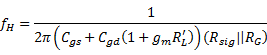
Low Frequency Cut-offs |
|
|
|
High Frequency Cut-offs
|
There
are three cut-off frequencies here |
There are two capacitances which cause high frequency gain roll-off. They are wiring capacitance and inter-electrode capacitance.
Wiring
capacitance : Inter-electrode
capacitance :
The change in current gain with frequency is also responsible for high frequency gain roll-off. This cut off is given by
|


Relation between gain bandwidth ![]() product
and
product
and ![]()
·
![]()
|
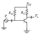
Fixed Bias |
|
|
|
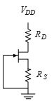
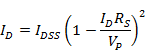
Self-Bias |
|
|
|
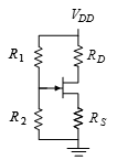
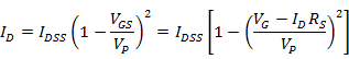
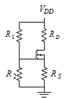
Voltage Divider Bias |
|
|
|
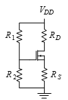
Depletion Type Voltage Divider Bias |
|
|
|
Enhancement Type Voltage Divider Bias |
|
|
|
Enhancement Type Drain Feedback Bias |
|
|
|
|
|
|
|
|
Transconductance |
Channel conductance |
||||
|
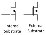
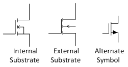
MOSFET |
|
|
||||
|
JFET |
|
|
![]() , called the device
parameter =
, called the device
parameter = ![]()
|
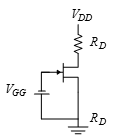
Common source Fixed Bias |
|
|
|
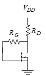
Common source Drain Feedback |
|
|
|
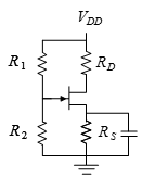
Common source Self-Bias with
unbypassed |
|
|
|
Common source Voltage
Divider with bypassed |
|
|
|
Common drain (Source Follower) |
|
|
|
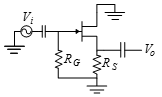
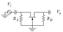
Common gate |
|
|

|
Common Source |
|
|
||||||
|
Common Source |
|
|
||||||
|
Common Drain |
|
|
||||||
|
Common Gate |
|
|


|
Input Impedance |
|
|
|
Output Impedance |
|
|
|
Current Gain |
|
|
|
Voltage Gain |
|
|
|
Overall Gain |
|
|


|
|
|
|
|
|
|
|
Depletion Type |
Enhancement Type |
|
n-MOS |
|
|
|
p-MOS |
|
|


|
|
|


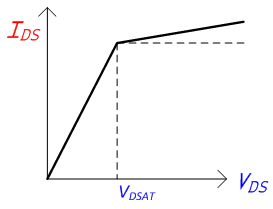
Conditions
necessary for saturation: ![]()
|
Current in linear (triode) region |
|
|
Current in saturation |
|
|
Process transconductance parameter |
|
|
Transconductance
|
|
|
Resistance |
|
|
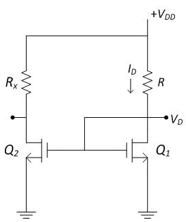
The mosfet in this schematic is always in saturation
|
The maximum
value of
|
|
Both the mosfets are identical
The minimum
voltage source
|
|


|
N-MOSFET Enhancement Type |
|
N-mosfet
enhancement type TURNS-ON when gate voltage is greater than
|
||||||
|
P-MOSFET Enhancement Type |
|
P-mosfet
enhancement type TURNS-ON when gate voltage is lesser than
|
||||||
|
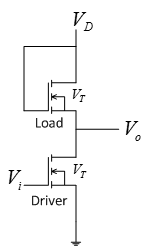
N-MOSFET Enhancement Type (Driver-Load) Inverter |
|
Load is always ON operating in saturation because gate is tied to the drain.
When When
In this arrangement power consumption is more than CMOS inverter because Load is always ON .
Note that in CMOS inverter drains are tied together whereas here drain and source are tied together. |
||||||
|
CMOS Inverter |
|
Load is a P-mosfet enhancement type device while Driver is an N-mosfet enhancement type.
When
When
It is not necessary that threshold voltage of the Driver and the Load be same |


|
|
|
|
|
|


|
No channel width modulation
|
Effect on
current due to channel width modulation and introduction of process parameter
|
|
Early voltage
and determination of
|
Finite output resistance due to channel width modulation
|


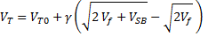
The effect of body effect is that the threshold voltage is reduced
![]() and
and ![]() are process parameters and
are process parameters and ![]() is the
is the
![]() when
when ![]() is
zero.
is
zero.
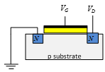
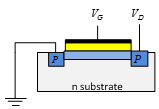
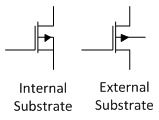
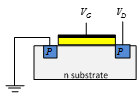
In an n-MOS device the substrate is connected to the most negative
voltage in the system so as to keep ![]() negative.
negative.
Drain current decreases with increase in temperature unlike BJT
There are three kinds of breakdown in mosfet
1. Breakdown of drain and substrate region due to high drain voltage. This is avalanche breakdown
2. If the channel width is small the depletion region at drain may cross the channel and overlap with the region at source. This causes increase in the drain current. This is called punch-through.
3. Breakdown of gate-oxide if static charge is deposited at the gate. This causes permanent damage.
|
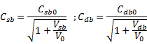
Capacitances in Mosfet |
Example |


|
Triode Region |
|
|
|
Saturation Region |
|
|
|
Cut off |
|
|
|
Unity gain bandwidth frequency |
|
|
|
Upper cut off frequency |
|
|
|
|
|
|
|
Q. Find
|
|
|
|


|
|
Assuming
|
|
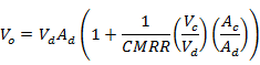
Common-mode Rejection Ratio |
|
|
|
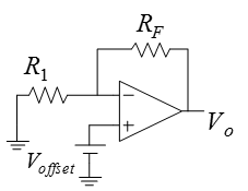
Input Offset- Voltage
|
|
Effect on output voltage due to input offset voltage
|
|
Input Offset- Current |
|
Effect on output voltage due to input offset current |
|
Input Bias- Current |
|
Relationship between Input bias current and Input offset current |
|
Slew Rate |
|
|
|
Cut off frequency |
|
Relation between open loop gain, gain-bandwidth frequency and the cut-off frequency |
|
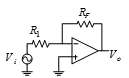
Inverting amplifier |
|
|
|
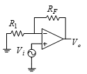
Non-inverting amplifier |
|
|
|
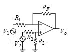
Subtract |
|
|
|
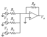
Summing Amplifier |
|
|
|
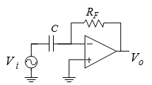
Integrator |
|
|
|
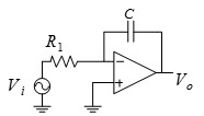
Differentiator |
|
|
|
Instrumentation Amplifier |
|
|

|
|
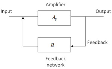
Feedback
factor =![]()
Overall
gain with feedback ![]()
|
Type of feedback |
Input Impedance |
Output Impedance |
|
Voltage-Series feedback |
Increases |
Decreases |
|
Voltage-Shunt feedback |
Decreases |
Decreases |
|
Current-Series feedback |
Increases |
Increases |
|
Current-Shunt feedback |
Decreases |
Increases |
‘Series’ increases Input impedance while 'Shunt' decreases it.
'Current' increases output impedance while ‘Voltage’ decreases it
|
Voltage Series Feedback
|
|
|
|
Current Series Feedback
|
|
|
|
Voltage Shunt Feedback
|
|
|


